

TSMC’s A14 Process Targets a Major SRAM Cell Size Reduction
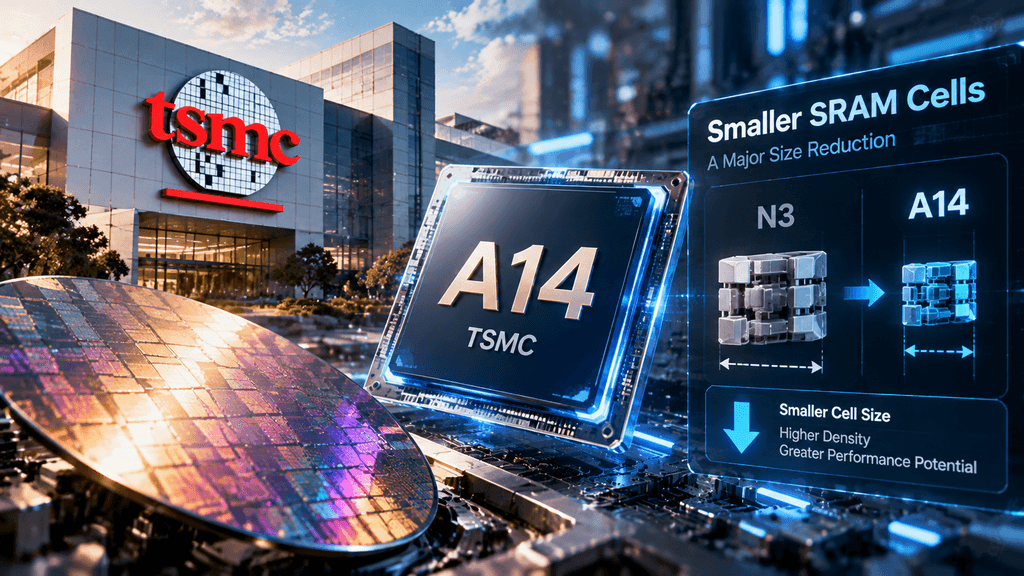
Semiconductor manufacturing has long treated SRAM scaling as a critical but stubborn challenge. For more than half a decade, logic transistor advanced while the high-density six-transistor SRAM bitcell that forms on-chip caches remained essentially fixed in size. That imbalance forced designers of CPUs, GPUs, and AI accelerators to devote ever-larger fractions of expensive die area to memory. TSMC’s upcoming A14 node, scheduled for volume production in 2028, is positioned to break the pattern. Company papers and recent industry reports indicate the high-density SRAM cell will drop below 0.017 square micrometers, representing a reduction of more than 19 percent from the approximately 0.021 µm² cell that has been standard since the N5 process entered production in 2020.
The advance will be detailed at the 2026 International Electron Devices Meeting in December under the NanoFlex Pro platform. By delivering the first meaningful high-density SRAM cell shrink in eight years alongside projected 10–15 percent speed gains or 25–30 percent power reductions and roughly 20 percent higher overall chip density versus N2, TSMC’s A14 process restores balance between logic and cache scaling at a moment when AI and high-performance computing workloads place unprecedented demands on on-chip memory capacity and efficiency.
Eight Years of Fixed SRAM Dimensions Forced Costly Design Compromises Across Nodes
From the introduction of N5 in 2020 through N3 variants and the current N2 nanosheet generation, TSMC’s high-density 6T SRAM bitcell area stayed locked near 0.021 µm². Logic density continued to improve, yet the memory cells that store frequently accessed data did not shrink in proportion. As a result, cache arrays consumed a rising share of total silicon area and wafer cost on successive process nodes. Designers responded by stacking additional cache dies, moving larger last-level caches onto separate, lower-cost chiplets, or accepting higher power and latency penalties from increased off-chip memory traffic. AMD’s X3D processors illustrate one response: extra L3 capacity placed on a stacked die to address the density limitations of the main compute die.
GPU architects and AI accelerator teams faced similar constraints when trying to enlarge on-chip SRAM buffers that reduce reliance on slower external high-bandwidth memory. The stagnation was not absolute, array-level density still rose modestly through better bitline organization and periphery layout on N2, but the fundamental cell size remained unchanged. That long plateau made any genuine reduction in bitcell area strategically important. Reports from late October 2026 confirm that A14 finally moves the number, targeting a cell smaller than 0.017 µm² and thereby reopening a path for more cache within the same footprint or the same cache in less silicon.
Exact Bitcell Area Targets Confirm More Than 19 Percent Reduction From Long-Standing Baseline
Public disclosures and the IEDM abstract place the A14 high-density SRAM cell at less than 0.017 µm². Relative to the 0.021 µm² reference used since N5, the reduction exceeds 19 percent; some calculations based on the upper bound of the new figure show theoretical cell-level density gains approaching 23–24 percent. TSMC attributes the improvement primarily to dimensional ground-rule scaling rather than a complete architectural redesign of the six-transistor cell itself. The company also claims the resulting SRAM macros will achieve the highest density reported to date. These figures appear in the abstract of a paper authored by Shien-Yang Wu and Chih-Hao Chang and scheduled for presentation on 14 December 2026.
Independent reports from multiple outlets in the final days of October 2026 consistently cites the same numbers and the same comparison to the N5-era cell. It is important to distinguish the published bitcell area from the effective density of a finished memory macro. Sense amplifiers, decoders, word-line drivers, and test circuitry occupy additional area, so the net improvement in usable cache density will be lower than the raw cell shrink. Even so, the directional change after eight years of stasis is substantial for any product whose performance is limited by on-chip memory capacity.
Cache Scaling Now Influences Die Economics as Strongly as Transistor Density Itself
Modern high-performance and AI chips devote a large and growing fraction of their area to SRAM. When the cell size stops shrinking while logic continues to densify, the relative cost of cache rises. That dynamic has already driven architectural decisions such as multi-die cache stacking and chiplet-based memory hierarchies. A cell that is more than 19 percent smaller reverses the trend. Design teams can either expand cache capacity within a fixed die budget or free area for additional compute, interconnect, or specialized accelerators.
For AI training and inference accelerators, larger on-chip SRAM reduces the frequency of expensive trips to external memory, improving both throughput and energy efficiency. Mobile and client SoCs benefit similarly by packing more L2 or L3 capacity into power-constrained footprints. The economic impact is magnified by the high cost of leading-edge wafers. Even a modest reduction in the silicon area required for a given cache size improves the number of good dies per wafer or allows more aggressive binning. Industry observers note that the timing coincides with continued growth in model sizes and data-movement intensity, making the SRAM improvement particularly relevant for products that will enter the market after 2028.
Full-Node PPA Gains Combine Logic Improvements With the New SRAM Density
TSMC positions A14 as a complete node transition relative to N2. Official targets include a 10–15 percent increase in speed at the same power or a 25–30 percent reduction in power at the same speed, together with an approximate 20 percent rise in overall chip density. The density figure is driven by both logic standard-cell innovations under the NanoFlex Pro architecture and the SRAM cell shrink. Second-generation nanosheet transistors form the foundation, refined from the first-generation devices introduced on N2. Standard-cell height and track-height optimizations further contribute to the area reduction. Packaging-related features are also part of the platform: through-silicon vias, an advanced redistribution layer supporting a 4.5 µm SoIC bond pitch, and high-performance metal-insulator-metal capacitors.
These elements are intended to ease system-level integration for multi-die products. The combination of transistor-level, cell-level, and packaging advances is what TSMC describes as a full-node power-performance-area improvement. Early internal test vehicles have already demonstrated device performance near 90 percent of target and 256 Mb SRAM yields approaching 90 percent, according to company comments in mid-2026 earnings discussions that have been reiterated in recent reporting.
Pilot-Stage Yields and Customer Engagement Indicate Steady Progress Toward Risk Production
By the middle of 2026, TSMC reported that product-like test vehicles on A14 had reached roughly 90 percent of targeted device performance and that 256 Mb SRAM structures showed yields close to the same level. Customer engagement for both smartphone and high-performance computing applications was described as active, with some design work progressing ahead of earlier internal schedules. Pilot production activity is under way to validate the node and to give customers silicon for design verification. Risk production is scheduled for 2027, with high-volume manufacturing targeted for 2028.
The IEDM abstract explicitly states that the technology remains on track for that volume-production date. Yield figures at this stage are measured on relatively simple test structures rather than full customer products, so further maturation will be required. Nevertheless, the reported numbers and the absence of public schedule slips suggest that the development program has avoided major technical roadblocks so far. Capacity planning points to significant wafer starts once volume ramps, with multiple fabs expected to contribute.
A14 Advances Beyond Rival Nodes in SRAM Scaling Metrics
Intel’s 18A process has publicly disclosed a high-density SRAM cell size of 0.021 µm², the same figure TSMC has used since N5, and a macro density of up to 38.1 Mb/mm² reported at an earlier conference. Samsung has not released comparable cell-size data for its most recent nodes. If the A14 cell below 0.017 µm² is realized in production, TSMC would hold a clear numerical lead in high-density SRAM area at the 2028 timeframe. Intel’s subsequent 14A node is positioned as competitive on overall density, yet specific SRAM cell figures for that process have not been published.
The comparison remains incomplete until production silicon and full macro characterizations appear, but the directional advantage in the published bitcell number is unambiguous. Foundry customers evaluating long-term roadmaps for cache-heavy designs will weigh this metric alongside performance, power, yield, and cost. The SRAM gap, if sustained, could influence decisions for products that require large on-chip memory arrays.
AI Accelerators Stand to Gain Directly From Higher On-Chip SRAM Capacity
Large language models and other AI workloads generate intense pressure on memory bandwidth and capacity. On-chip SRAM provides the lowest-latency, lowest-energy storage for activations, weights, and intermediate results. When that SRAM cannot scale with compute, accelerators become more dependent on external HBM or DDR, increasing both power and latency. A reduction of more than 19 percent in bitcell area allows designers either to enlarge the SRAM budget within the same die outline or to reclaim area for additional compute units or higher interconnect bandwidth.
The effect is multiplicative: more local memory improves utilization of the available arithmetic units and reduces the energy cost per operation. TSMC’s own messaging positions A14 for HPC and AI applications in addition to mobile SoCs. Early customer interest in those segments has already been noted. The practical outcome will depend on how efficiently the periphery circuits scale and on the voltages and currents required by the production macros, yet the direction of the cell-size change aligns with the needs of the market.
Macro Density Ultimately Depends on Scaling of Supporting Circuitry Alongside the Bitcell
A smaller bitcell is only the first step. Complete SRAM macros contain address decoders, sense amplifiers, write drivers, column multiplexers, and built-in self-test logic. These periphery blocks have historically scaled more slowly than the array itself. TSMC states that dimensional ground-rule scaling enables the highest macro density reported to date, implying concurrent improvement in the supporting circuitry. Independent commentary has noted that bit-cell height reductions on the order of 16 percent and optimized periphery layouts contribute to the overall result.
Designers must still verify that the high-density cell can meet the access-time and voltage requirements of different cache levels. Fast L1 and L2 caches often employ larger, higher-current cells than the densest high-density cell quoted in technology papers. The published number therefore represents an upper bound on density rather than a guarantee for every memory instance on a chip. Still, the availability of a meaningfully smaller high-density option expands the design space for capacity-critical blocks.
Advanced Packaging Elements Extend the Reach of the A14 Platform Beyond the Die
The A14 NanoFlex Pro description includes several packaging and integration features. Through-silicon vias, an innovative redistribution layer that supports a 4.5 µm SoIC bond pitch, and high-performance MiM capacitors are listed as enablers for system-level scaling. These elements facilitate tighter multi-die assemblies and improved power delivery or decoupling within advanced packages. For products that already combine compute dies with separate cache or HBM stacks, the finer bond pitch and improved interconnect options can reduce latency and increase bandwidth between components.
The first version of A14 retains conventional front-side power delivery; a later Super Power Rail backside-power variant is expected roughly a year afterward. High-power desktop and data-center parts may therefore wait for the backside-power revision, while mobile and lower-power designs can adopt the initial platform. The packaging roadmap reinforces the view of A14 as a system technology rather than solely a transistor-scaling node.
Clear Milestones Stretch From Current Pilot Work Through 2027 Risk Production to 2028 Volume
A14 remains in the pilot and customer-evaluation phase. Risk production is planned for 2027, followed by volume manufacturing in 2028. The IEDM abstract confirms the volume-production target. Internal test results from mid-2026 showed device performance and SRAM yields near 90 percent of goal, providing confidence that the schedule is realistic. Some market commentary has speculated about a possible modest acceleration, yet TSMC has not officially advanced the high-volume date.
Fab construction and tool installation continue in support of the ramp, with capacity expected to reach tens of thousands of wafers per month once production is established. The multi-year runway allows customers time to complete design work, qualify the process, and prepare software and system enablement. Products built on A14 are therefore unlikely to appear in volume before 2029, giving the industry a predictable window in which to plan around the new density and performance envelope.
Future Cache Hierarchies in CPUs and GPUs Can Expand Without Proportional Die Growth
With a smaller high-density cell available, architects can reconsider the balance among L1, L2, L3, and specialized scratchpad memories. Larger last-level caches become more affordable in terms of silicon area, potentially reducing the need for aggressive multi-die stacking solely for capacity reasons. GPU designs that already allocate substantial area to local memory can increase buffer sizes or free transistors for additional streaming multiprocessors. The net effect is greater flexibility in the performance-versus-cost trade-off.
Because A14 wafers will remain expensive, the economic benefit will appear most clearly in products that previously hit hard area limits. Early adopters in the AI and high-performance segments are expected to exploit the extra density first, followed by broader adoption as the process matures and costs decline. The eight-year gap since the last meaningful cell shrink means many existing design methodologies were built around a static cell size; those methodologies will now be updated to take advantage of the new baseline.
Production Realities Will Determine How Closely Silicon Matches Conference Numbers
Conference bitcell figures are measured on optimized test structures under controlled conditions. Production macros must satisfy a wider range of voltage, temperature, and reliability requirements while coexisting with logic transistors and complex interconnect. Assist circuits, redundancy, and yield-enhancement features add area that is not reflected in the pure cell size. High-current cells used for speed-critical caches remain larger than the densest high-density cell. Wafer cost will be high in the early years of the node, so the absolute cost of cache may not fall as quickly as the density rises.
These caveats are standard for any new process technology and do not diminish the importance of the reported shrink. They simply set expectations that the full system-level benefit will emerge gradually as design teams, IP providers, and foundry process engineers refine the implementation. Monitoring of actual product die photographs, macro density disclosures, and customer comments after 2028 will provide the ultimate verification.
December IEDM Session Will Supply the First Detailed Technical Description of the Platform
The paper titled “A14 CMOS NanoFlex Pro Platform Technology with 2nd Gen. Nano-sheet and Full Node PPA Benefits for HPC/AI and Mobile SoC Applications” is scheduled for the afternoon of 14 December 2026. Authors from TSMC will present the SRAM cell results, the density claims, the performance and power targets, and the supporting packaging features. Conference papers typically contain more quantitative data, process cross-sections, and electrical characterization than the short abstract that is already public.
Industry participants will examine the measured versus targeted numbers, the variability of the new cell, and any discussion of production readiness. The presentation will also allow direct comparison with concurrent papers from other foundries. Until that session, the available information rests on the abstract, company roadmap statements, and consistent secondary reporting from late October 2026. The IEDM talk is therefore the next major public checkpoint for the A14 SRAM story.
FAQs
What exactly is the reported size of the A14 high-density SRAM cell and how does it compare with earlier nodes?
TSMC’s abstract and supporting reports state that the high-density 6T SRAM bitcell will measure less than 0.017 µm². The same cell has measured approximately 0.021 µm² from the N5 process introduced in 2020 through N3E and N2. The reduction therefore exceeds 19 percent in area, corresponding to a theoretical increase of more than 23 percent in the number of cells that can fit in a given silicon area before periphery overhead is considered.
When will A14 reach volume production and when might the first products appear?
Volume manufacturing is targeted for 2028. Risk production is planned for 2027. Because of the normal lag between process qualification and product design completion, shipping products built on A14 are not expected in volume before 2029.
How do the performance and power targets of A14 compare with N2?
At the same power, A14 is projected to deliver 10–15 percent higher speed. At the same speed, power consumption is projected to fall 25–30 percent. Overall chip density is expected to rise by roughly 20 percent through the combined effects of logic and SRAM scaling.
Does a smaller bitcell automatically translate into 19 percent more cache on a finished chip?
No. The periphery circuits that surround the array, decoders, sense amplifiers, and related logic, occupy additional area and may not scale at exactly the same rate. The net macro density gain will therefore be lower than the raw cell-area reduction, although TSMC claims the highest macro density reported to date.
How does the A14 SRAM cell compare with Intel’s disclosed figures?
Intel’s 18A high-density cell is listed at 0.021 µm², matching the size TSMC has used since N5. If the A14 cell remains below 0.017 µm² in production, TSMC will hold a numerical advantage in that specific metric at the relevant timeframe.
Why has SRAM scaling lagged logic scaling for so long?
The six-transistor cell is sensitive to process variation, leakage, and stability at low voltages. Maintaining adequate noise margins and write ability while continuing to shrink the transistors has proven more difficult than scaling pure logic devices, leading to the multi-year plateau observed after N5.
Disclaimer: This general market information, possibly from third-party, commercial, or sponsored sources, is provided for reference and educational purposes only and does not constitute financial or investment advice, an offer, solicitation, or guarantee. We disclaim liability for its accuracy, completeness, reliability, and any resulting losses. Investments/trading are risky; past performance doesn’t guarantee future results. Users should research, judge prudently, and take full responsibility. For further details, please consult KuCoin’s Terms of Use and Risk Disclosure.